Camera Wafer Defect Inspection and Pasting

Solution brief

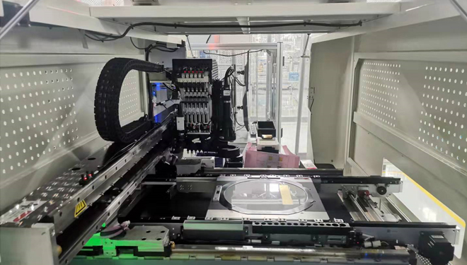
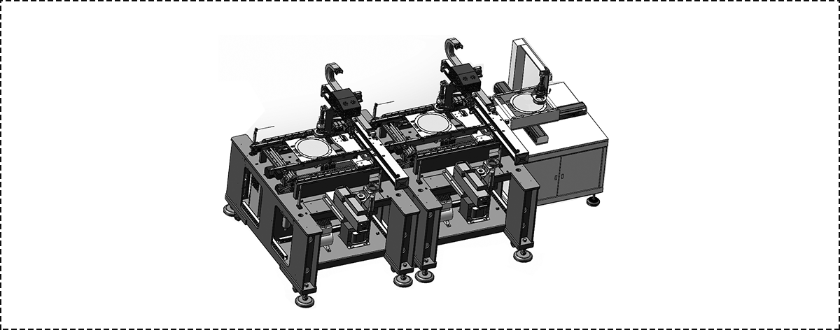
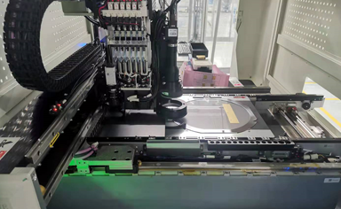
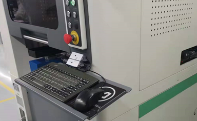
The solution based on AI computer vision can inspect wafer defects and dimensions, and mounting good products onto PVC disk according to certain angle, position, pitch and direction, and outputting eMap file containing position, angle and other information for downstream manufacturers' production use. The wafer is a copper wafer of size 0.9*0.81mm, and it needs to inspect both front and back sides. Because of the small size of wafer and high CT requirement, so it is completed by using placement machine with optical inspection.


Solution function

Based on the model library of the TimesAI deep learning development platform, the inspection of micro disordered components is achieved, and high-speed and high-precision disk swing/placement is completed.

Bright spot

1. Adopt deep learning to achieve product defect inspection, which is more intelligent and accurate; 2. The mounting machine achieves high-precision and high-speed mounting, providing equipment productivity; 3. Reverse detection achieves high-speed flying photography, minimizing CT; 4. Vibrating disc loading, reducing labor participation, and saving costs; 5. Automatically generate eMap files to identify product coordinates, detection results, angles, and other data, providing automation basis for downstream manufacturers

Application scenario

Product case

  • Scenario

  • Scenario

  • Scenario